Data sheets for electronic components include a lot of parameter specifications and it is quite common to see minimum, maximum, and typical values. Intuitively, the typical values represent the most frequently occurring cases, while the min and max values present the limits. The difference between typical values and min/max values is sometimes quite big. This can be quite important when designing electronic circuits. For example, what if you design for the typical value—but when manufacturing your device you encounter parts closer to the min/max limits? Will your device still function as expected?
To avoid any min/max value surprises, it’s a good idea to design for the min/max specs, not the typical specs. Doing so, however, can make your product a bit over-designed, or at least more expensive than it should be. Often data sheets don’t even list min/max specs which makes it even more confusing. It is good to have a good understanding of how the typical and min/max values are defined and measured but—apart from the intuitive understanding mentioned above—I had not seen a good concise description.
Typical Specifications and Distributions
While reading the data sheet of the Texas Instruments TLV9151 opamp I stumbled upon section 7.3.8, which does a pretty good job explaining how typical and min/max specs are defined and how they should be used. I copied the relevant information below—or you can refer to the PDF data sheet.
Designers often have questions about a typical specification of an amplifier in order to design a more robust circuit. Due to natural variation in process technology and manufacturing procedures, every specification of an amplifier will exhibit some amount of deviation from the ideal value, like an amplifier’s input offset voltage. These deviations often follow Gaussian (“bell curve”), or normal distributions, and circuit designers can leverage this information to guardband their system, even when there is not a minimum or maximum specification in the Electrical Characteristics table.
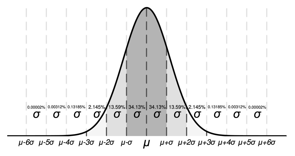
The figure above shows an example distribution, where μ, or mu, is the mean of the distribution, and where σ, or sigma, is the standard deviation of a system. For a specification that exhibits this kind of distribution, approximately two-thirds (68.26%) of all units can be expected to have a value within one standard deviation, or one sigma, of the mean (from μ – σ to μ + σ).
Depending on the specification, values listed in the typical column of the Electrical Characteristics table are represented in different ways. As a general rule of thumb, if a specification naturally has a nonzero mean (for example, like gain bandwidth), then the typical value is equal to the mean (μ). However, if a specification naturally has a mean near zero (like input offset voltage), then the typical value is equal to the mean plus one standard deviation (μ + σ) in order to most accurately represent the typical value.
You can use this chart to calculate approximate probability of a specification in a unit; for example, for TLV915x, the typical input voltage offset is 125 μV, so 68.2% of all TLV915x devices are expected to have an offset from -125 μV to +125 μV. At 4 σ (±500 μV), 99.9937% of the distribution has an offset voltage less than ±500 μV, which means 0.0063% of the population is outside of these limits, which corresponds to about 1 in 15873 units.
Specifications with a value in the minimum or maximum column are assured by TI, and units outside these limits will be removed from production material. For example, the TLV915x family has a maximum offset voltage of 675 μV at 25°C, and even though this corresponds to about 5 σ (≈1 in 1.7 million units), which is extremely unlikely, TI assures that any unit with larger offset than 675 μV will be removed from production material.
For specifications with no value in the minimum or maximum column, consider selecting a sigma value of sufficient guardband for your application, and design worst-case conditions using this value. For example, the 6-σ value corresponds to about 1 in 500 million units, which is an extremely unlikely chance, and could be an option as a wide guardband to design a system around. In this case, the TLV915x family does not have a maximum or minimum for offset voltage drift, but based on the typical value of 0.3 μV/°C in the Electrical Characteristics table, it can be calculated that the 6 σ value for offset voltage drift is about 1.8 μV/°C. When designing for worst-case system conditions, this value can be used to estimate the worst possible offset across temperature without having an actual minimum or maximum value.
Hopefully the information above clarifies some of the questions about typical and min/max specs of electronic components.